25. Sample-and-hold circuits
We have performed analog-to-digital conversion (ADC) in earlier lessons. But let’s think about what that entails for a moment. ADC involves taking an analog voltage and, ideally, instantaneously converting the voltage to a set of bits. (The ADCs built in to Arduino Uno are 10-bit.) The conversion is not instantaneous, though. The input voltage used for ADC has to be held constant for some time to enable ADC complete its process. (There are many ways of doing ADC; see section 13.5 of Horowitz and Hill for a discussion.)
Sample-and-hold circuits are designed for this purpose. Given a sampled voltage, a sample-and-hold circuit holds that voltage, usually so that it can be measured or used for some other purpose.
Basic sample-and-hold architecture
The essential components of a sample-and-hold circuit are two unit-gain amplifiers, a switch, and a capacitor, shown in the schematic below.

The left op-amp serves to make a replica of the input, but after the op-amp, the input has very low impedance. Imagine that the open switch is now closed (ON). As charge builds up in the capacitor, the voltage across it grows. When the switch opens (OFF), whatever charge that has accumulated in the capacitor is held because the right op-amp does not allow current to flow through its input terminals. Thus, the voltage across the capacitor is held until the switch is closed again; the charge has nowhere to go. The voltage across the capacitor is the input voltage to the right op-amp. Since the op-amp has unit gain, its output voltage is the held voltage in the capacitor.
So, the “sample” step involves turning the switch on and building up the charge of the capacitor so that the voltage across the capacitor matches the input voltage. The “hold” step involves turning the switch off and outputting the held capacitor voltage.
The choice of capacitance \(C\) depends on the goals of the sample-and-hold circuit. If you need to hold the voltage for a long time, you want a large \(C\), since you will lose voltage across the capacitor according to \(\mathrm{d}V/\mathrm{d}t = I_\mathrm{leak}/C\), where \(I_\mathrm{leak}\) is the current that leaks through the right op-amp. (Such drop in voltage while holding is called droop.) On the other hand, if you want to have high frequency sampling, you need to be able to charge up the capacitor quickly, so you want \(C\) to be small. Furthermore, there is some finite resistance in the switch, so the capacitor is part of a low-pass filter. So, you want \(C\) to be small so that high frequency signals are not filtered out.
Follow-along exercise 16: Building a sample-and-hold circuit
In most applications, the switch is a metal-oxide-semiconductor field-effect transistor (MOSFET). For this exercise, you will instead build a sample-and-hold circuit using an npn BJT as the switch.
Build the sample-and-hold circuit below using one of your LF412CP dual op-amp integrated circuits. You can power the op-amps with a ±5 V Digilent PowerBRICK or with the BE 189 shield.

To demonstrate how sample-and-hold works, you will use the MCP4725 DAC to supply a sinusoidally varying voltage ranging from zero to 3.3 V with a frequency of 1 Hz. You will obtain a voltage from the DAC and from the output of the sample-and-hold circuit every 10 ms. Use a hold time of 100 ms in the sample-and-hold circuit.
If you like, you can use the Arduino sketch below and use the Serial Plotter of the Arduino IDE or serial-dashboard to see the signal that comes out of the DAC (to pin A0) and the signal that comes out of the sample-and-hold circuit (to pin A1). Otherwise, you can build a Bokeh app to monitor the result (and possibly control things like hold times, frequency, etc.).
#include <Adafruit_MCP4725.h>

#define MCP4725_ADDR 0x62

const int sampleAndHoldSwitchPin = 2;
const int analogOutPin = A0;
const int sampleAndHoldPin = A1;

const float freq = 1;
const unsigned long sampleDelay = 10;
const unsigned long sampleAndHoldDelay = 100;
unsigned long lastSampleTime = 0;
unsigned long lastSampleAndHoldTime = 0;

Adafruit_MCP4725 dac;


void setup() {
  //
  pinMode(sampleAndHoldSwitchPin, OUTPUT);
  pinMode(sampleAndHoldSwitchPin, HIGH);

  dac.begin(MCP4725_ADDR);

  Serial.begin(115200);
}


void loop() {
  unsigned long currTime = millis();
  if (currTime - lastSampleTime > sampleDelay) {
    // Set output voltage
    uint16_t x = (uint16_t)(2703 * (1 + sin(2 * PI * freq * millis() / 1000.0)) / 2.0);
    dac.setVoltage(x, false);

    lastSampleTime = currTime;

    // Make sure we are in hold mode
    digitalWrite(sampleAndHoldSwitchPin, LOW);

    // Read
    int dacReading = analogRead(analogOutPin);
    int sampleAndHoldReading = analogRead(sampleAndHoldPin);

    Serial.print(dacReading);
    Serial.print(" ");
    Serial.println(sampleAndHoldReading);

    if (currTime - lastSampleAndHoldTime > sampleAndHoldDelay) {
      // Switch to sample mode
      digitalWrite(sampleAndHoldSwitchPin, HIGH);
      lastSampleAndHoldTime = currTime;
    }
  }
}
When you look at the plot, you can see that the sample-and-hold circuit indeed obtains a sample and then holds the voltage at that level until sampling again.
The LF398N integrated circuit
We have LF398N sample-and-hold integrated circuits. These are widely used sample-and-hold components. They work much as the circuit you have built above, but naturally have some optimizations.
The pinout for the LF398N integrated circuit is shown below.
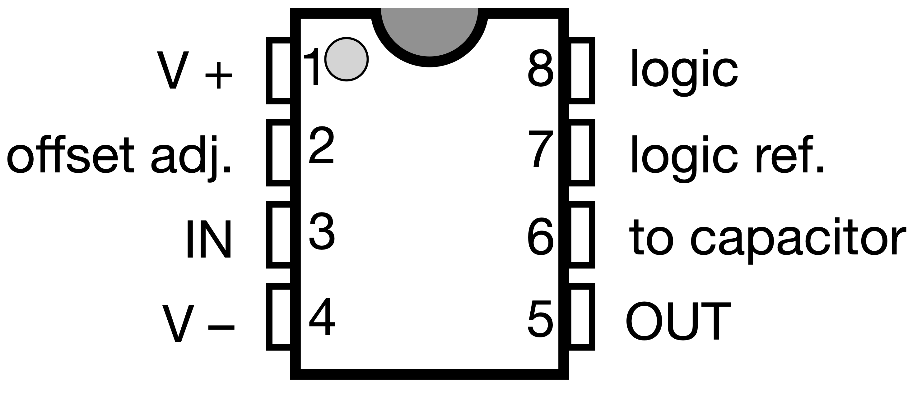
The V+ and V- pins are connected to power supplies and may accept ±5 V up to ± 18 V. The offset adjustment pin compensates for any DC offsets (you should not need to connect that pin). The input and output pins are self-explanatory. Pin 6 in the pinout connects to the holding capacitor, which is then connected to ground. You can use this pin to use a capacitor with capacitance that is best for your application. The logic pin is used to open and close the switch. If the voltage across the logic pin is higher than that of the logic reference pin, the switch is on, and if the voltage across the logic pin is lower than that of the logic reference pin, the switch is off. You should choose how to control the logic depending on your application. For example, if you are going to turn the switch in the sample-and-hold on and off using an Arduino digital pin, which can write zero or five volts, you might want to use a voltage divider to connect 2.5 V to the logic reference pin. On the other hand, if you are going to be switching between positive and negative voltages for your logic, you should connect the logic reference pin to ground.
Do-it-yourself exercise 12: Using the LF398N for sample-and-hold
Now perform sample-and-hold using the LF398N integrated circuit using a similar circuit as above. That is, swap out the hand-built sample-and-hold circuit above with one using LF398N. You can even just add LF398N-based sample-and-hold to that circuit if you wish. Generate similar plots either using the Serial Plotter in the Arduino IDE, serial-dashboard, or with a custom Bokeh app.